Business
Laser Annealing
Laser Annealing for Semiconductor
Laser Annealing for Semiconductor
- VisAA offers optimal laser annealing processes that are required where conventional annealing tool is unable to fulfill the performance.
- Multi-wavelength system provides precise control of annealing depth and continuous wave laser irradiation performs gentle annealing
treatment without affecting neighboring structure.
-
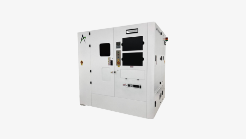
VisAA (Visible-laser Activation Anneal) / VisMA (Visible-laser Melting Anneal)
Multi Function Wafer Annealing Machine
- Fine activation process: Diffusion-free, excellent Rs uniformity
- Anneal depth control via multiple wavelength laser
- Single or multiple wavelengths simultaneous irradiation on demand
- Smooth roughness after annealing
- Multi-wavelength optimized optics, precision stage and small foot print
-
Application
- Wafer Ion Implant Activation Process
- Void Remover to DRAM Deep Trench Structure Reflow Process
Main Specifications
| Item | Specification | |
|---|---|---|
| System | Semiconductor wafer annealing system by laser beam irradiation | |
| System configuration |
1) Laser & Optics system 2) Stage 3) Heating chuck system 4) Alignment & Monitoring system 5) Operating software |
|
| System Size |
Approximated size: 2,440(W) x 1,920(D) x ≤ 2500(H) Approximated weight: 4ton |
|
| Available workpiece |
Material : 200mm wafer Thickness : <1mm |
|
| Installation Environment | Temp/Humidity |
Temperature control ≤ ±2℃ Humidity control 55% ± 10% |
| Clean room | Class 1000 | |
| Vibration | VC-C | |
| Laser | R-G-B Laser | |
| Optics |
Beam mode : Rectangular flat-top Beam size : >160x100µm² / >800x500µm² Power density : >2x10⁵W/cm² (RGB each) / >8x10³W/cm² (RGB each) |
|
| Heating chuck |
Heater Power : 208V, 1,770W Available Temp. : 380 °C (Max : 400 °C) |
|
| Stage | X, Y, Z and θ axis | |
| Accuracy | ≤ ±1μm | |
| Software function |
Recipe editor Wafer alignment Leveled user access control Data logging |
|
| Alignment | Lens magnification | 2X, 10X |
Process performance
-
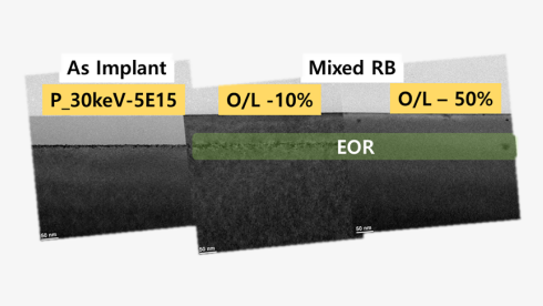 Dopant Activation Process
-
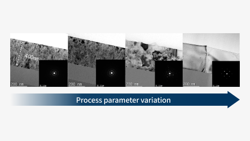 Void Melting Process