Business
Advanced Laser Process Development
Precision laser process
-
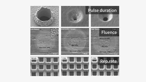
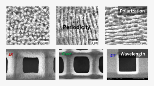
Features
- Pulse duration
- Pulse energy/fluence
- Repetition rate
- Polarization
- Wavelength
- Aggregated set of parameters with unique process strategy for sub-micron level precision processing
-
Application
- Non-thermal metal/polymer/glass patterning and cutting
- Precision filter / masking devices
Fine Laser Patterning
- fs Laser : Cold ablation by ultrashort pulse duration
- Mask projection : Finely controlled beam shaping
- Unique process : Theraml effect management process
Target material
 Metal(Invar 36)
-
Organic material(Polyimide)
-
Inorganic material(Glass)
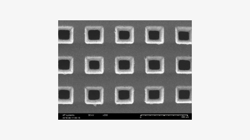
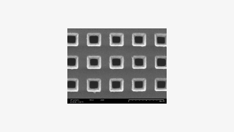
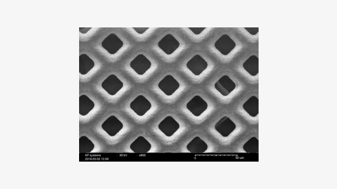
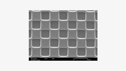
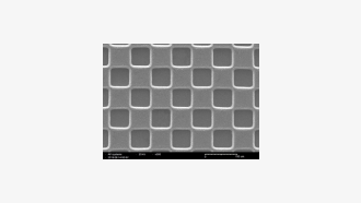
Various process
-
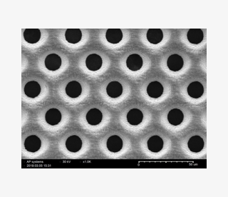
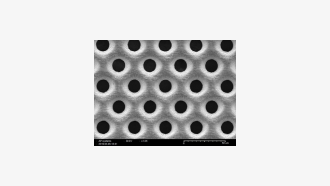 Fine patterning
-
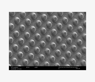
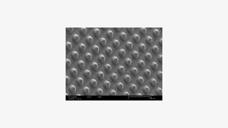 Embossing patterning
-
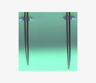
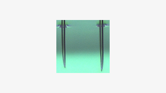 High aspect ratio drilling
Semiconductor laser annealing
-
Features
- Appropriate wavelength selection for various layers
- Optimum process strategy
- Optimum optics configuration
- Proper monitoring tools
-
Application
- Activation anneal after implantation
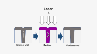
- Void Removal within DRAMŌĆÖs trench Structure
- Silicidation
- Crystallization
- Complete melting by suitable laser is a fine solution for void removal of trench structure
- Selection of wavelength and process parameters, successful process achieved
-
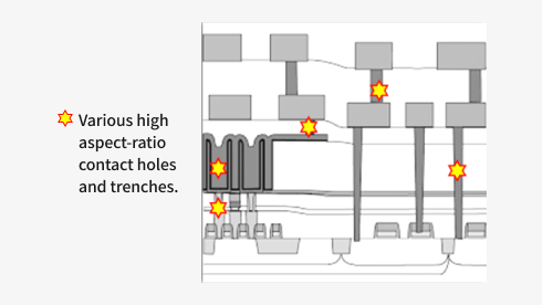
Cross Sectional View of Typical DRAM Device
-
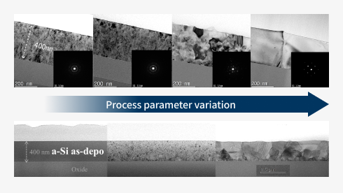
Process parameter variation
Concept of melting annealing

- Dopant activation by laser would be needed when device dimension gets finer
- Fine activation result achieved by selection of wavelength and process parameters
- Amount of dopant diffusion is negligible compared to conventional RTA process
-
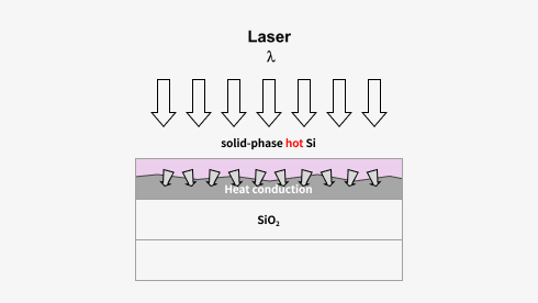 Non-melting process mechanism :
Solid phase transition -
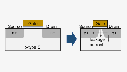 Limitation of conventional annealing ;
leakage current followed by diffusion
Process Performance
-
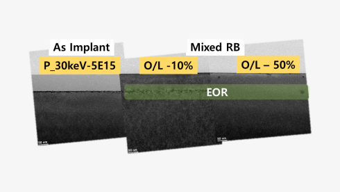 Clearnace of defect including EOR
-
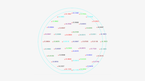 Uniformity of Sheet Resistance :
StdDev/ave ~ 0.307%
Improved wafer surface roughness
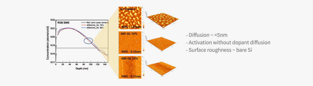
- Diffusion ~ <5nm
- Activation without dopant diffusion
- Surface roughness ~ bare Si